Research
Vision
Computing is spreading from the Internet of Things toward an Internet of Everything, and silicon cannot follow it everywhere. A silicon chip takes a long time and enormous cost to bring into production, and it has to be built on a rigid surface — a poor fit for surfaces that bend, or for devices meant to be ubiquitous, item-level consumer electronics.
We build the technology that fills that gap: low-cost, high-performance electronics and intelligent sensors that can be made quickly, over large areas, and on almost any surface. Our approach starts with the material and works upward, in three stages.
01Design the material
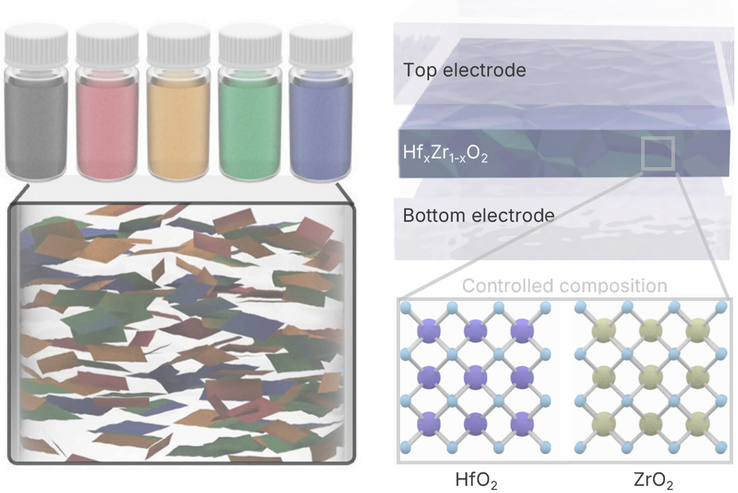
Every electronic device is built from three kinds of materials: conductors that carry current, semiconductors that switch it, and insulators that block it. We design and synthesize all three ourselves as nanomaterials, and our goal is to engineer their properties at the atomic scale.
For example, controlling the stoichiometry, ion incorporation, and composition of a dielectric layer1–3, or the defect density and heterojunction design of a semiconducting channel4,5, lets us tune the electrical and optical characteristics of the material itself. We are now extending this design space toward finer control — over local composition, crystalline phase, and the interfaces between layers — in order to develop exotic material properties that conventional thin films do not offer.
02Make it at scale
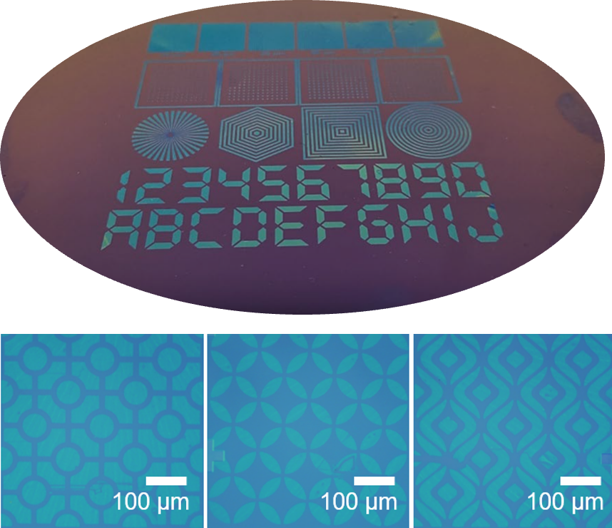
A material is only useful if it can be produced uniformly and reproducibly across an entire wafer. To achieve this, we first disperse atomically thin (van der Waals) materials into high-quality inks with a variety of electronic properties5. These inks can be integrated into a range of solution-based processes, including spin-coating, slot-die printing, and inkjet printing2,6, which makes the platform low-cost and scalable, with deposition completed across a full wafer in a matter of seconds. Together, these steps let us produce high-quality van der Waals thin films over wafer-scale areas.
Printing covers flat surfaces well, and some applications additionally require integration into three-dimensional structures, capacitors being one example. For these, we use atomic layer deposition to grow the designed material one atomic layer at a time, so that it conforms to deep, high-aspect-ratio trenches3. Printing for planar, large-area integration and ALD for three-dimensional integration together provide the process building blocks that a printed electronics platform requires.
03Build the device
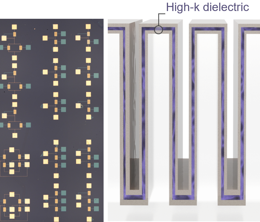
Using these scalable films, we develop advanced fabrication processes, such as photopatterning7, to build high-performance transistor and photodetector arrays over large areas2. We also work on next-generation devices, including retina-inspired neuromorphic sensors and optoelectronic synapses4,8,9, using the same printed films. These have generally been demonstrated with complex device structures such as multiple gate terminals; we obtain them from structurally simple devices instead, letting the material properties we design at the atomic scale supply the behavior that would otherwise come from the device architecture.
The three-dimensional structured films then serve a different purpose: next-generation capacitors that move past the limits of planar geometry — far more active area within the same footprint, and correspondingly higher charge storage3.
Our ultimate goal is to bring these devices together into a complete device platform: switching, sensing, and storage in a single working system, built end to end from the materials and processes we develop ourselves.
Looking ahead
These three axes converge on one thing: a printed electronics platform. What the Internet of Everything needs is electronics cheap enough to put anywhere, in the right form factor, and good enough to be worth putting there. That is what we are building.
References
- Kim, K.†, Kim, J.† et al. Sub-stoichiometric zirconium oxide as a solution-processed dielectric for reconfigurable electronics. Nat. Electron. 8, 461–473 (2025).
- Kwon, Y. A.†, Kim, J.† et al. Wafer-scale transistor arrays fabricated using slot-die printing of molybdenum disulfide and sodium-embedded alumina. Nat. Electron. 6, 443–450 (2023).
- Cheema, S. S. et al. Giant energy storage and power density negative capacitance superlattices. Nature 629, 803–809 (2024).
- Kim, J. et al. Multilevel optical programming of intrinsic vacancies in solution-processed MoS2 films for retinomorphic color differentiation. Adv. Opt. Mater. (2026).
- Kim, J. et al. All-solution-processed van der Waals heterostructures for wafer-scale electronics. Adv. Mater. 34, 2106110 (2022).
- Song, O., Rhee, D., Kim, J. et al. All inkjet-printed electronics based on electrochemically exfoliated two-dimensional metal, semiconductor, and dielectric. npj 2D Mater. Appl. 6, 64 (2022).
- Kwak, I. C.†, Kim, J.† et al. Orthogonal photopatterning of two-dimensional percolated network films for wafer-scale heterostructures. Nat. Electron. 8, 235–243 (2025).
- Kim, J. et al. Multicolor optoelectronic synapse enabled by photon-modulated remote doping in solution-processed van der Waals heterostructures. Adv. Funct. Mater. (2025).
- Nam, K.†, Kim, J.†, Ji, S.† et al. Light-induced field-tunneling synapses in solution-processed van der Waals heterostructures for scalable, retina-inspired optical sensing. Adv. Funct. Mater. (2026).